You know Apple, NVIDIA and AMD. Chances are you have a product designed by one of them within arm’s reach. The name of the company that physically manufactures their most advanced processors probably means far less to you: Taiwan Semiconductor Manufacturing Company, or TSMC.
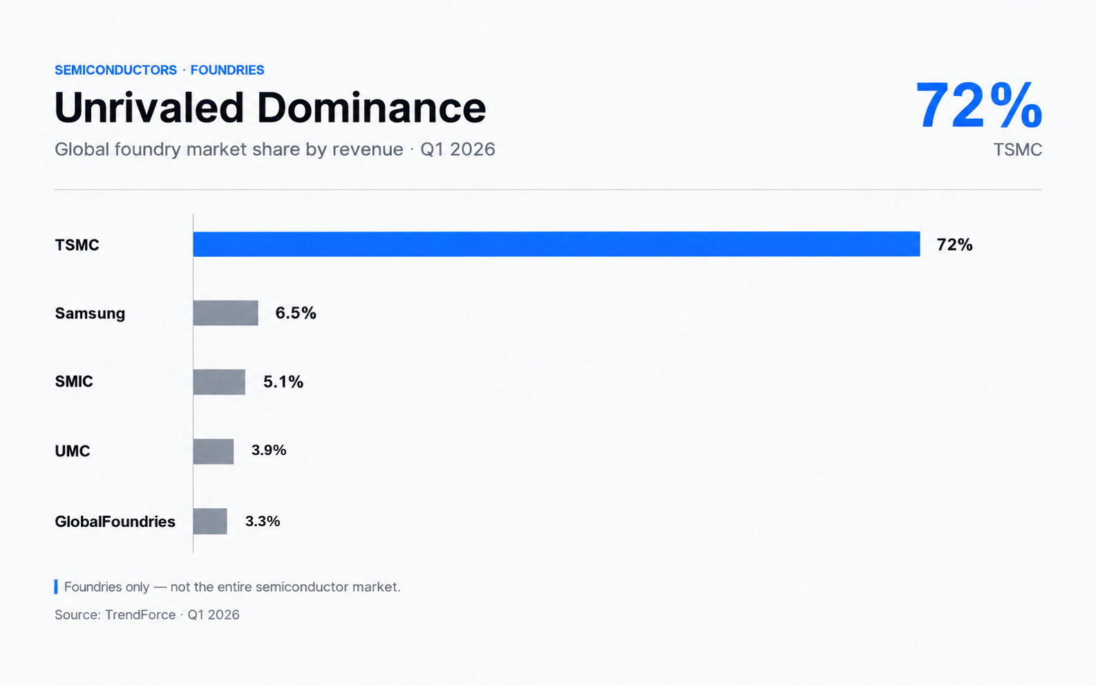
That is the paradox of this Taiwanese company. Barely part of the public’s vocabulary, it has become an almost unavoidable gateway for modern computing. In the first quarter of 2026, TSMC held about 72% of the global foundry market, measured by revenue, according to research firm TrendForce, a share that rose to 72.5% in the second quarter. A rival firm, Counterpoint, using a slightly different scope, puts it at about 73% in the second quarter of 2026.
That figure needs an immediate clarification. 72% does not mean that TSMC makes 72% of the world’s chips. It is the company’s share of the foundry market — companies that manufacture chips on behalf of other businesses — measured by revenue.
How did a company that most people have never heard of become this chokepoint? The answer is not a technology that no one else could understand. It lies in a choice of business model made nearly forty years ago, and in everything that choice has allowed TSMC to accumulate since.
Explainer — 72%, but 72% of what?
Two markets are often confused. The foundry market — companies that manufacture chips for third parties — where TSMC accounted for about 72% of revenue in the first quarter of 2026 (TrendForce). And the semiconductor market as a whole — which includes memory, analog chips and sensors, largely produced by other companies — where TSMC is far from a majority. Neither measure says that “TSMC makes most of the world’s chips.”
The idea that changed the semiconductor industry
In 1987, Morris Chang founded TSMC in Hsinchu, Taiwan. Its initial capital, about $220 million, came almost half from the Taiwanese government’s Development Fund and a little over a quarter from the Dutch group Philips.
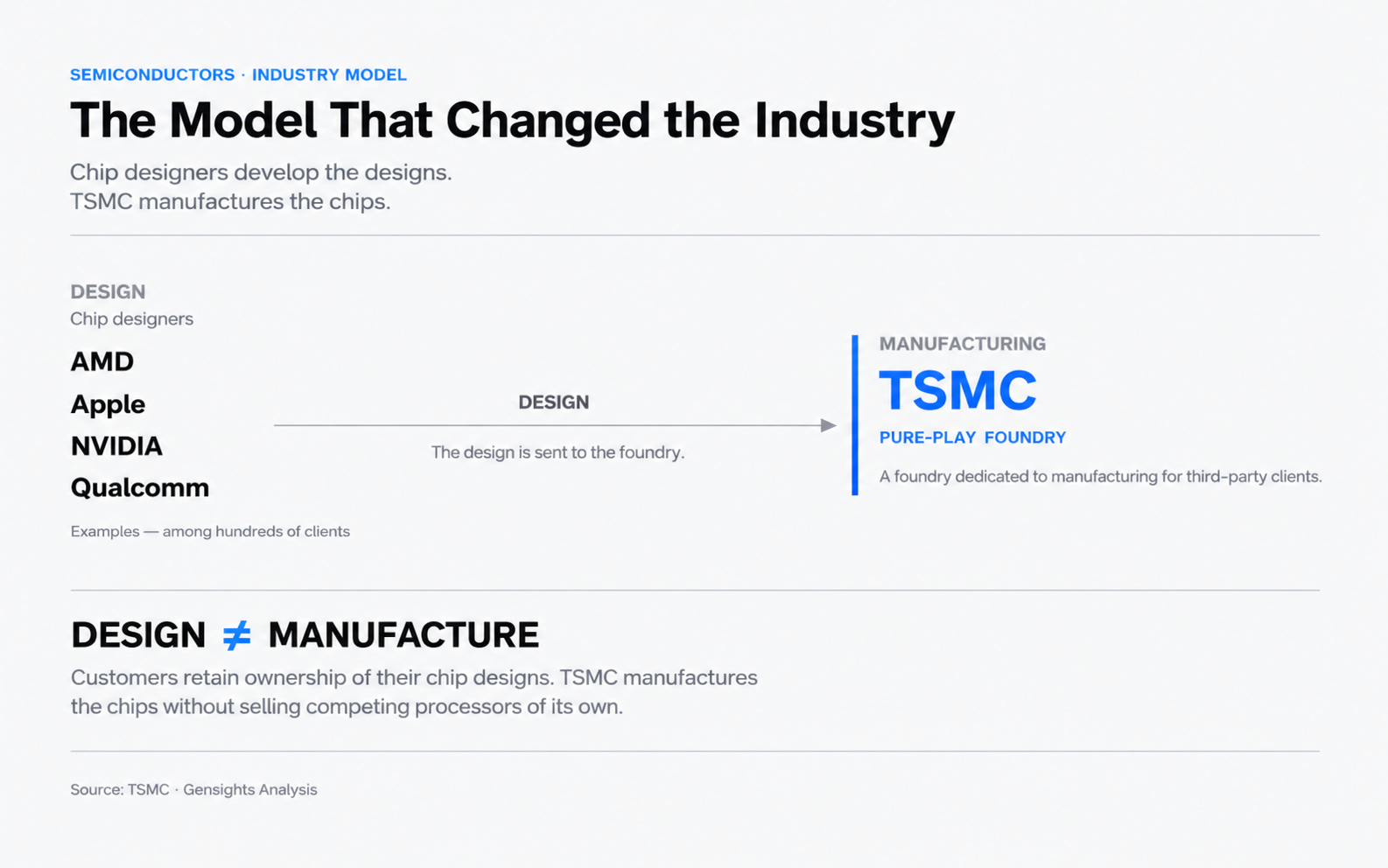
Chang’s idea fits in one sentence: TSMC would only manufacture chips, and only for other companies. It would never design a circuit under its own brand, never sell a finished product, never compete with its customers. Today the company describes itself as “the world’s first dedicated semiconductor foundry” and says it “pioneered the pure-play foundry business model.”
The wording matters: TSMC did not invent contract manufacturing — integrated manufacturers were already renting out some of their spare capacity. What it popularized was the pure-play model: a company whose only business is manufacturing for others.
That detail changes everything. An integrated device manufacturer — an IDM, such as Intel or Samsung — designs its own chips and owns its fabs. When it manufactures for a third party, that third party is often a competitor of its own design division: are the customer’s designs guaranteed to stay confidential? When capacity is tight, who gets served first? A pure-play foundry has no design division. The conflict disappears.
That neutrality made possible the ecosystem of so-called fabless companies — those that design and sell chips without owning a single fab. By relying on a neutral foundry, a young company could access cutting-edge manufacturing without tying up tens of billions of dollars in concrete and equipment.
Explainer — Fab, fabless, foundry
A fab is a chip manufacturing plant. A fabless company (“without a fab”) designs and sells chips but manufactures none: NVIDIA, AMD, Qualcomm, or Apple for its processors. A foundry does the opposite: it manufactures, on behalf of third parties, chips it did not design. An IDM does both — it designs and manufactures: Intel, Samsung.
How TSMC became the manufacturer for tech’s giants
Today, the most visible chips in the technology industry are designed by fabless companies and manufactured by TSMC.
Apple designs the processors in its iPhones (A series) and Macs (M series) itself; it owns no fabs. TSMC manufactures them — the A19 and A19 Pro chips in the 2025 iPhones are made on its 3 nm process. This point is often misunderstood: TSMC designs nothing for Apple. It executes designs that Apple provides. (For how Apple turns that design work into value, see our analysis “How Apple Became a $4 Trillion Company.”)
The pattern is the same for NVIDIA, which designs the graphics processors at the heart of artificial intelligence servers and has TSMC manufacture them; for AMD, which builds its processors from small assembled blocks — chiplets — that TSMC produces; and for Qualcomm, whose Snapdragon chips are now mostly made by TSMC, after a split with Samsung that has varied from one generation to the next.
In 2025, NVIDIA became TSMC’s largest customer. TSMC does not name its customers, but its 2025 annual report shows that its largest customer — identified as NVIDIA — accounted for 19% of revenue, ahead of its second-largest, Apple (17%). Together, the two represent roughly a third of the foundry’s revenue; its ten largest customers, 78%, or nearly four-fifths.
These companies do not spread their orders across several manufacturers, because switching foundries is not an ordinary purchasing decision. A new processor is co-optimized with a specific process years before it launches; switching means going back to that stage, at the risk of lower yields and a less competitive product. The result is mutual lock-in: the customer depends on the foundry, and the foundry plans its fabs around the volumes its major customers commit to.
Why a $20 billion fab is not enough
If the advantage came down to equipment, any player with enough capital could buy a fab, fill it with tools and catch up with the foundry. Why doesn’t that work?
Start with the equipment. Extreme ultraviolet (EUV) lithography, essential for the most advanced processes, is made by only one company in the world: the Dutch firm ASML. An EUV machine costs on the order of $150 million to $200 million; the next generation, known as High-NA, about €350 million. But TSMC, Samsung and Intel all have access to ASML’s EUV tools — and Samsung and Intel even deployed High-NA before TSMC, which has said it will bring this generation into volume manufacturing only from 2030, once the tools are mature and their cost reasonable. If TSMC’s lead came from privileged access to equipment, it would not exist.
The advantage lies in what TSMC does with those machines. Making an advanced chip requires several thousand process steps, chained in a precise order, each tuned with proprietary recipes that the foundry constantly refines: this is process integration — not a machine, but the way hundreds of operations combine to deliver, at the end of the line, a majority of working chips.
That share of usable chips on a wafer — the yield — determines the cost per chip and the volume that can be delivered. And yield cannot be bought: it improves as a process matures — through defect analysis, statistical control and continuous recipe adjustment. High-volume production generates more data to find those defects and stabilize the process faster; it is this accumulated learning that drives yield, not volume in itself. A newcomer that produces less and discovers its processes later starts with a handicap that is hard to close. That is the reasoning that led GlobalFoundries to abandon a 7 nm process in 2018: the cost of the leading edge was no longer sustainable for a company of its size. That left only three companies at the leading edge: Intel, Samsung and TSMC.
Add to this teams able to stabilize these processes over several generations — know-how built over years — an ecosystem of critical suppliers beyond ASML (etch and deposition equipment, photoresists, ultra-pure gases), and patient capital: TSMC spent about $40 billion on capital expenditures in 2025 and now plans $60 billion to $64 billion in 2026, a range it reaffirmed in October 2026 after spending about $40.6 billion in the first nine months of the year. A single advanced-process fab costs tens of billions of dollars, most of it in equipment — an entry ticket that rises with every generation.
Replicating TSMC is therefore not a matter of buying a fab and some machines. It would also mean replicating decades of industrial learning — while the foundry keeps moving ahead.
Explainer — Why ASML is not enough
ASML is the world’s only maker of EUV lithography machines, but TSMC, Samsung and Intel all have access to them. TSMC is even adopting the next generation (High-NA) after its competitors. Its advantage therefore does not come from privileged access to equipment, but from process integration — thousands of co-optimized steps — and from accumulated industrial learning.
The real moat against Samsung and Intel
TSMC is not alone at the leading edge. Two players have, on paper, a process in the same class.
Samsung runs a sizable foundry business — about 6% of the market — and was even the first, in 2022, to adopt the newest transistor architecture. It launched its 2 nm process in 2025 and won orders, including from Tesla for its self-driving chips. Press and analyst reports, however, have pointed to difficulties in ramping yields on its advanced processes, with no official data allowing a quantified comparison with TSMC.
Intel, for its part, has made its foundry the key to its industrial survival. Its 2 nm-class process, called 18A, has been in volume production since late 2025 and makes Intel’s own processors. On the foundry side, external traction on this node remains limited. For the next generation, 14A, still in development, Tesla has said it intends to use Intel’s process for some of its future AI chips; Intel says it is in talks with potential customers without naming them publicly. 14A production is expected around 2028. The turnaround of its foundry is therefore neither assured nor ruled out.
The point is not that Intel or Samsung are “X years behind” — no metric supports that claim. It is that having a comparable process is not enough: it also takes stabilized yields, flawless execution across several generations, an order book filled by external customers, and the scale to fund the next generation. TSMC meets these conditions today — a 2 nm process in volume production, demand that management says still far exceeds what it can supply, an established fabless customer base and the capacity to invest. It is their combination, more than any single technological lead, that forms the moat.
The world has created a single point of concentration
This success has a hidden side, and it is geographic.
Leading-edge manufacturing remains heavily concentrated in Taiwan. TSMC’s own schedule shows it: its 3 nm and 2 nm processes, the most advanced it produces in volume, are manufactured only in Taiwan today, and the first 3 nm volume production outside the island is not expected before the third quarter of 2027, in Arizona. A disproportionate share of the world’s most advanced chips comes out of a handful of large Taiwanese industrial hubs, notably Hsinchu, Tainan and Taichung.
This concentration creates concrete risks. Taiwan is an earthquake zone: a magnitude 7.4 earthquake in April 2024 briefly halted some TSMC lines. The fabs also consume huge amounts of ultra-pure water and electricity, on an island that went through a drought in 2021 that forced rationing. Add the tensions between China and Taiwan, which make this concentration a national security issue for several major powers.
This is the context in which the idea of a “silicon shield” emerged, debated since the early 2000s. The idea: Taiwan’s central role in semiconductors would protect it, either because China’s own economy depends on these chips, or because the United States and its allies would have an interest in defending the island. It is a strategic interpretation, contested, not a guarantee: several analysts — including historian Chris Miller, author of Chip War — argue that such a “shield” would not deter an invasion, and that building fabs abroad could even weaken its logic.
The world did not choose to depend on TSMC. It chose to stop manufacturing for itself — and TSMC filled the gap.
Arizona, Japan, Germany: can TSMC be decentralized?
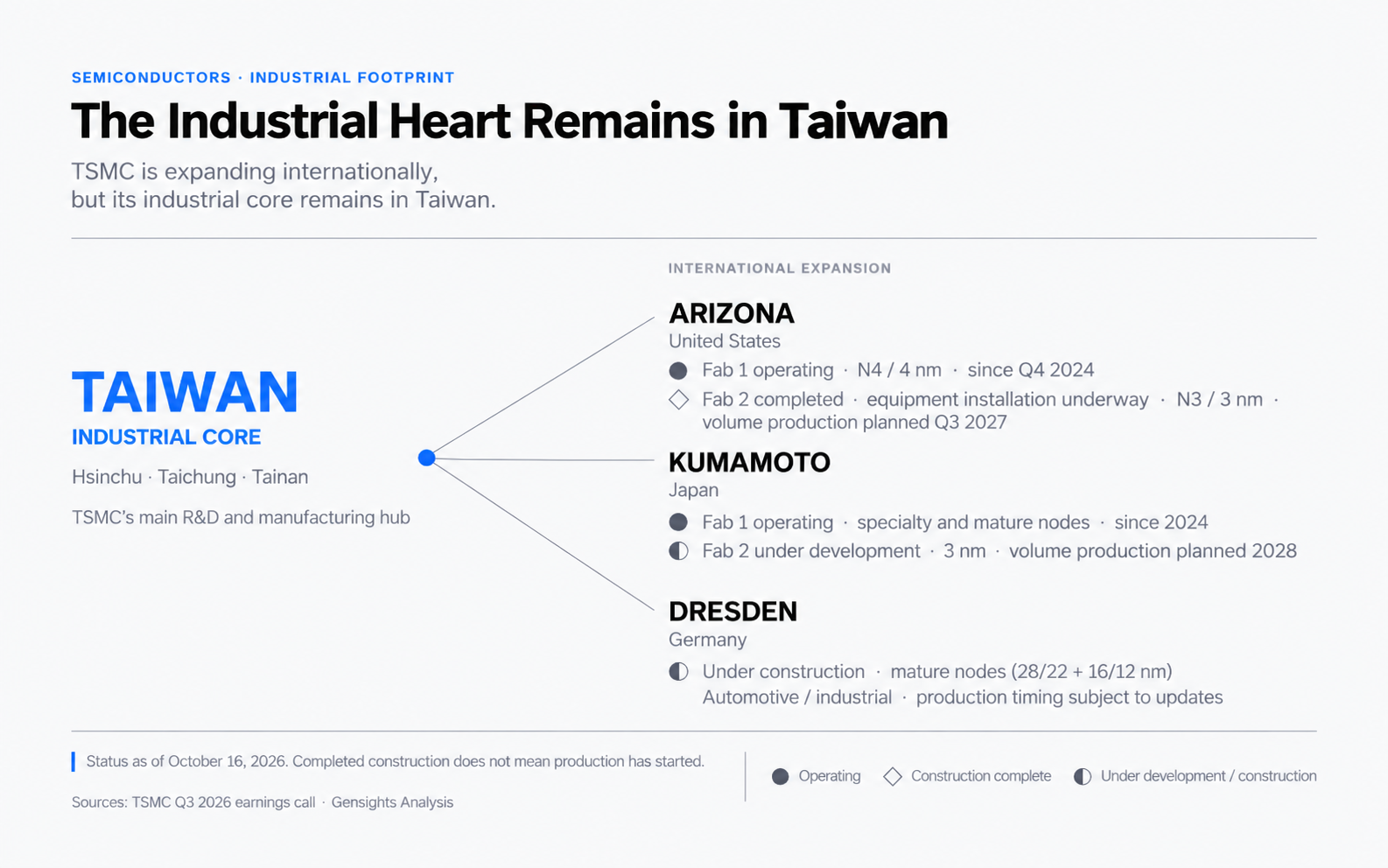
Since 2020, TSMC has been building outside Taiwan. Three projects, three different situations.
Arizona. The total announced amount has been raised several times — from about $12 billion in 2020 to about $265 billion in 2026. It covers six wafer fabs, two advanced packaging facilities and an R&D center, plus several additional fabs for 2 nm and more advanced processes announced in July 2026. It is a total of successive announcements, a plan spread over more than a decade: neither money already committed nor money already spent. So far, only one fab is operational, on a 4 nm process — one generation behind Taiwan’s leading edge — for customers such as Apple, NVIDIA and AMD. The second fab, whose construction is complete, is being fitted with tools and is due to start 3 nm volume production in the third quarter of 2027; the following fabs, for 2 nm and beyond, are targeted by the end of the decade. U.S. public support (CHIPS Act) amounts to $6.6 billion in direct funding and up to $5 billion in loans.
Japan. In Kumamoto, the JASM joint venture — majority-owned by TSMC, with Sony, Denso and Toyota — has operated a first fab on mature processes (28 to 12 nm) since late 2024, which turned profitable in the first quarter of 2026. A second fab, originally planned for less advanced nodes, has been upgraded to 3 nm, with volume production planned for 2028.
Dresden. In Germany, the ESMC joint venture — majority-owned by TSMC, with Bosch, Infineon and NXP — is building a fab representing an investment of more than €10 billion, about half of it funded by the German state. It will produce mature processes (28 to 12 nm), mainly for the automotive and industrial sectors; the building was topped out in September 2026, the first process tools are due to be installed in the second half of 2027, and production is still announced for 2027 — neither a leading-edge site nor an operational one at this stage.
The key point: diversifying is not replacing. Dresden is not designed for the leading edge; Kumamoto will move closer to it with its second fab, planned for 3 nm, but not before 2028 under the current schedule. Arizona could produce leading-edge processes toward the end of the decade. In the short term, none of these sites manufactures at Taiwan’s scale.
Explainer — Announced is not operational
Announced: the total amount and the number of fabs (Arizona: ~$265B — six fabs, plus several more announced in July 2026 — a cumulative total of successive announcements). Awarded: the public support actually allocated (Arizona: $6.6B under the CHIPS Act). Under construction: most of the sites. Operational: a single fab in Arizona (4 nm process) and the first Kumamoto fab (mature nodes). Leading-edge production outside Taiwan is not expected before the end of the decade.
AI makes TSMC even more strategic
The artificial intelligence wave has tightened this dependence on two fronts at once.
The first is leading-edge manufacturing. The accelerators that train and run AI models — notably NVIDIA’s and AMD’s graphics processors — are made on TSMC’s most advanced processes. These advanced processes (7 nm and below) already accounted for 74% of the company’s wafer revenue in 2025, and 79% in the third quarter of 2026; the “high-performance computing” platform, which includes these chips, rose from 41% of revenue in 2022 to 68% in the third quarter of 2026.
The second front is more recent: advanced packaging. A modern AI accelerator is not a single chip but an assembly — a logic processor surrounded by stacks of high-bandwidth memory, connected on a shared substrate. TSMC performs this assembly with a process called CoWoS. Analyst estimates point to a rapid expansion of this capacity since 2024, while TSMC’s management says demand still far exceeds the supply it can provide; according to DigiTimes, NVIDIA has booked more than half of the expanded CoWoS capacity for 2026–2027.
AI’s bottleneck is therefore no longer just how finely chips can be etched: it is also the capacity to assemble these complex chips, an area where TSMC again has a lead that is hard to close quickly. Not all of AI depends on TSMC — some chips are made elsewhere. But the most advanced accelerators do, for both manufacturing and assembly.
Can TSMC stay indispensable?
TSMC’s position is strong, but it is not guaranteed.
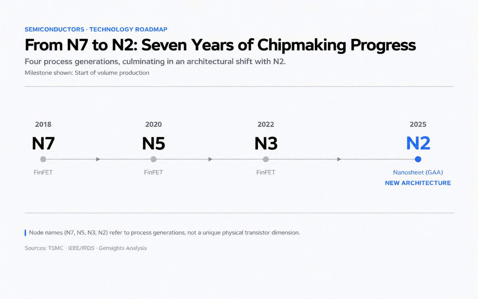
Its strengths. Its 2 nm process, in volume production since late 2025, introduces a new transistor architecture at TSMC — the nanosheet, or GAA, in which the gate wraps more fully around the transistor’s channel, improving its electrical control. Compared with the previous generation, TSMC cites a 10% to 15% performance gain, or a 25% to 30% reduction in power consumption. Management says demand for its leading-edge technologies still far exceeds what it can supply, and it now expects 2026 revenue to grow about 44% in U.S. dollar terms; its gross margin, close to 60% in 2025 and 66.4% in the third quarter of 2026, gives it the means to fund the next generation.
Its risks and uncertainties. The cost of each generation is rising; the competition, on paper, has moved closer; international expansion, more expensive to operate than the Taiwanese fabs, will weigh on profitability; and geopolitics remains a major unknown. The outcome will depend on how fast Intel and Samsung execute, on the trajectory of costs, on how tensions around Taiwan evolve, and on TSMC’s ability to turn its current volume into a future lead. None of these factors has a clear-cut answer today.
Conclusion
TSMC did not become indispensable because it holds a technology that no one else understands. Its competitors know the physics, buy the same machines and employ capable engineers.
What TSMC has accumulated, and what neither its customers nor its competitors can quickly rebuild, is a system: a model free of conflicts of interest, decades of yield learning, proprietary process integration, an ecosystem of suppliers, considerable capital, the trust of the largest chip designers — and now mastery of advanced packaging.
By gradually entrusting their manufacturing to this company, the technology giants were able to focus on design and avoid colossal investments. But collectively, they have created a single point of industrial concentration — one company, one island — on which the rest of the world now depends, and which it cannot replace within a few years.
Specialization made the world more efficient. It also made it dependent on a single place.
Key takeaways
- TSMC designs no chips: it manufactures those designed by others — Apple, NVIDIA, AMD, Qualcomm.
- Its ~72% market share refers to the foundry market, by revenue (Q1 2026) — not to all the chips in the world.
- Its lead does not come from exclusive access to equipment, but from process integration and industrial learning accumulated at scale.
- Leading-edge manufacturing remains highly concentrated in Taiwan; the fabs in Arizona, Japan and Germany diversify production but will not replace the island in the short term.
- Artificial intelligence deepens the dependence on two fronts: advanced manufacturing and packaging (CoWoS).
Glossary
The terms fab, fabless, foundry and IDM are defined in the explainer in the first section.
| Term | Definition |
|---|---|
| Node | The commercial name of a process generation (“5 nm,” “3 nm”). For about fifteen years, it has no longer been a measured physical dimension, but a class of density and performance. |
| Yield | The share of working chips obtained from a silicon wafer. It determines the cost per chip. |
| EUV | Extreme ultraviolet lithography, essential for advanced processes. The machines are made only by ASML. |
| GAA / nanosheet | A transistor architecture in which the gate wraps more fully around the channel, for better electrical control. Adopted by TSMC at the 2 nm node. |
| CoWoS | TSMC’s packaging process that combines a logic processor and high-bandwidth memory on a shared substrate. It has become central to AI accelerators. |
Sources
Sources actually used in the body, ranked by type. Volatile data revalidated as of October 16, 2026, including TSMC’s third-quarter 2026 results published on October 15, 2026.
Primary sources
- TSMC — About TSMC (corporate page). Accessed in 2026. https://www.tsmc.com/english/aboutTSMC
- TSMC — Fourth Quarter and Full Year 2025 Results (SEC, Form 6-K), January 2026; 2025 Annual Report on Form 20-F, April 2026. https://www.sec.gov/Archives/edgar/data/1046179/000104617926000008/a4q25e_withguidancexfinal.htm · https://investor.tsmc.com/sites/ir/sec-filings/2025_20F%20Report.pdf
- TSMC — 2026 Quarterly Results: second-quarter results and capital budget increase (July 2026); third-quarter results, management report and earnings conference transcript (October 15, 2026). https://investor.tsmc.com/english/quarterly-results/2026/q3
- TSMC — TSMC Arizona (official page). 2026. https://www.tsmc.com/static/abouttsmcaz/index.htm
- TSMC — Press release: TSMC Arizona and U.S. Department of Commerce Announce up to US$6.6 Billion in Proposed CHIPS Act Direct Funding. April 2024. https://pr.tsmc.com/english/news/3122
- U.S. Department of Commerce / NIST — Biden-Harris Administration Announces CHIPS Incentives Award with TSMC Arizona. November 2024. https://www.nist.gov/news-events/news/2024/11/biden-harris-administration-announces-chips-incentives-award-tsmc-arizona
- ESMC / TSMC — Press release: ESMC Breaks Ground on Dresden Fab. August 2024. https://pr.tsmc.com/english/news/3169; Focus Taiwan, Construction of TSMC fab in Germany on track: ESMC president, September 15, 2026. https://focustaiwan.tw/business/202609150007
Industry data
- TrendForce — Strong AI Demand and Early Consumer Electronics Inventory Build Drive Top 10 Foundries to 3.7% QoQ Revenue Growth in 1Q26 (June 12, 2026); Global Foundry Revenue Approaches US$53.49 Billion in 2Q26 as SMIC Narrows Market Share Gap with Samsung (September 9, 2026); Intel Tapped as Tesla Wins First 14A Customer Spot in Terafab Push (April 23, 2026). https://www.trendforce.com/presscenter/news/20260612-13095.html · https://www.trendforce.com/presscenter/news/20260909-13225.html · https://www.trendforce.com/news/2026/04/23/news-intel-tapped-as-tesla-wins-first-14a-customer-spot-in-terafab-push/
- Counterpoint Research — Global Pure Foundry Market Share (Quarterly). August 27, 2026. https://counterpointresearch.com/en/insights/global-semiconductor-foundry-market-share
- DigiTimes — TSMC expands CoWoS capacity with Nvidia booking over half for 2026-27. December 2025. https://www.digitimes.com/news/a20251210PD218/
- Silicon Canals — Advanced chips of 7 nanometers and beyond made up 74% of TSMC’s wafer revenue in 2025. June 2026. https://siliconcanals.com/j-v-advanced-chips-of-7-nanometers-and-beyond-made-up-74-of-tsmcs-wafer-revenue-in-2025/
Reference press
- Taiwan News — Nvidia overtakes Apple to become TSMC’s largest client. February 27, 2026. https://www.taiwannews.com.tw/news/6310676
- Taipei Times — TSMC’s Kumamoto fab swings to profit in Q1 (May 18, 2026); Taiwan government approves TSMC’s 3nm upgrade for second Japan fab (April 1, 2026). https://www.taipeitimes.com/News/front/archives/2026/05/18/2003857513 · https://www.taipeitimes.com/News/biz/archives/2026/04/01/2003854797
- Tom’s Hardware — Samsung’s fab roadmaps examined — Taylor, Pyeongtaek, and the yield woes behind a $16.5 billion Tesla deal. 2026. https://www.tomshardware.com/tech-industry/samsungs-fab-roadmap-examined
- Bits&Chips — TSMC confirms 3nm fab in Japan (February 5, 2026); Why is TSMC not in a rush to adopt high-NA EUV? (April 30, 2026). https://bits-chips.com/article/tsmc-confirms-3nm-fab-in-japan/ · https://bits-chips.com/article/why-is-tsmc-not-in-a-rush-to-adopt-high-na-euv/
- MIT Technology Review — Taiwan’s “silicon shield” could be weakening. August 2025. https://www.technologyreview.com/2025/08/15/1121358/taiwan-silicon-shield-tsmc-china-chip-manufacturing/
Technical / reference
- IEEE Spectrum — Morris Chang: Foundry Father; GlobalFoundries CTO on Why the Company Abandoned the “Bleeding Edge” (2018). https://spectrum.ieee.org/morris-chang-foundry-father · https://spectrum.ieee.org/globalfoundries-cto-on-why-the-company-abandoned-the-bleeding-edge
- Chris Miller — Chip War: The Fight for the World’s Most Critical Technology, 2022 (book).
(18 entries, several grouping more than one reference from the same publisher — primary sources first.)