The most advanced chips contain billions of transistors built at extraordinarily small dimensions.
But before those components can be manufactured, patterns must be reproduced on a silicon wafer to form the chip’s successive layers.
That is the role of lithography.
And for some of the most demanding layers in advanced chips, this process now depends on an exceptionally complex technology: extreme ultraviolet lithography, or EUV.
At the center of that technology stands ASML.
The Dutch company does not manufacture chips. Among other products, it builds the systems that allow semiconductor manufacturers to print patterns onto wafers.
But an EUV machine is not simply a more precise version of an earlier machine.
It must generate light that is difficult to produce, transport that light even though almost everything absorbs it, control it with extraordinarily precise optics, move components with minute accuracy and continuously correct imperfections throughout the system.
And it must do all of this quickly and reliably enough to operate in a factory.
That combination explains why ASML’s technology is so difficult to replicate.
ASML Does Not Manufacture Chips
A modern chip is built progressively on a silicon wafer.
At different stages of production, patterns must be transferred onto its surface. Lithography systems project those patterns onto a light-sensitive layer, allowing subsequent manufacturing steps to build the circuit.
ASML supplies machines that perform this stage.
It is important to distinguish two businesses.
Companies such as TSMC, Samsung and Intel operate the factories where chips are produced.
ASML supplies some of the equipment that makes this manufacturing possible.
The challenge examined here, then, is not how to manufacture an entire chip.
It is how to build one of the most complex tools required to make one.
And to understand why that tool has become so difficult to reproduce, we must start with light.
To Make Smaller Features, the Industry Had to Change the Light
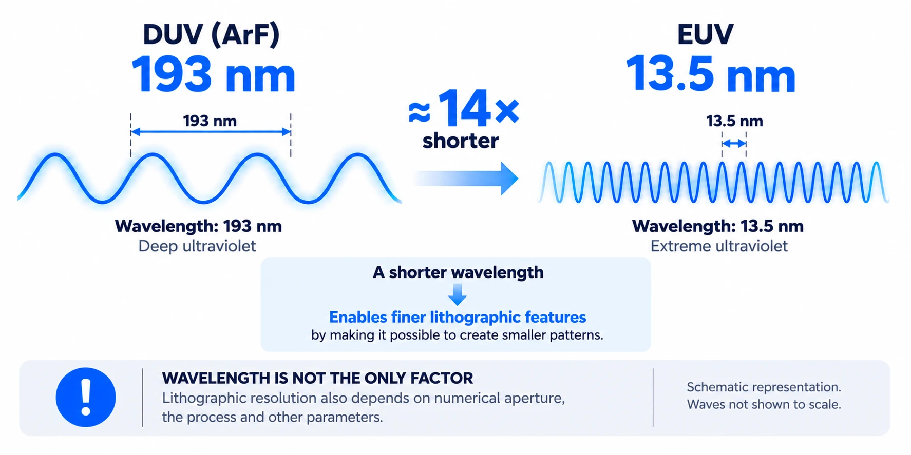
DUV systems using an argon fluoride (ArF) laser operate at a wavelength of:
193 nanometers.
EUV uses:
13.5 nanometers.
A wavelength more than fourteen times shorter.
That does not mean transistors automatically become fourteen times smaller. Lithographic resolution also depends on numerical aperture and other process parameters.
But a much shorter wavelength extends what lithography can achieve.
And this change immediately creates another challenge.
There is no simple EUV lamp that can be installed inside the machine.
The light itself must be generated.
First, the EUV Light Must Be Generated
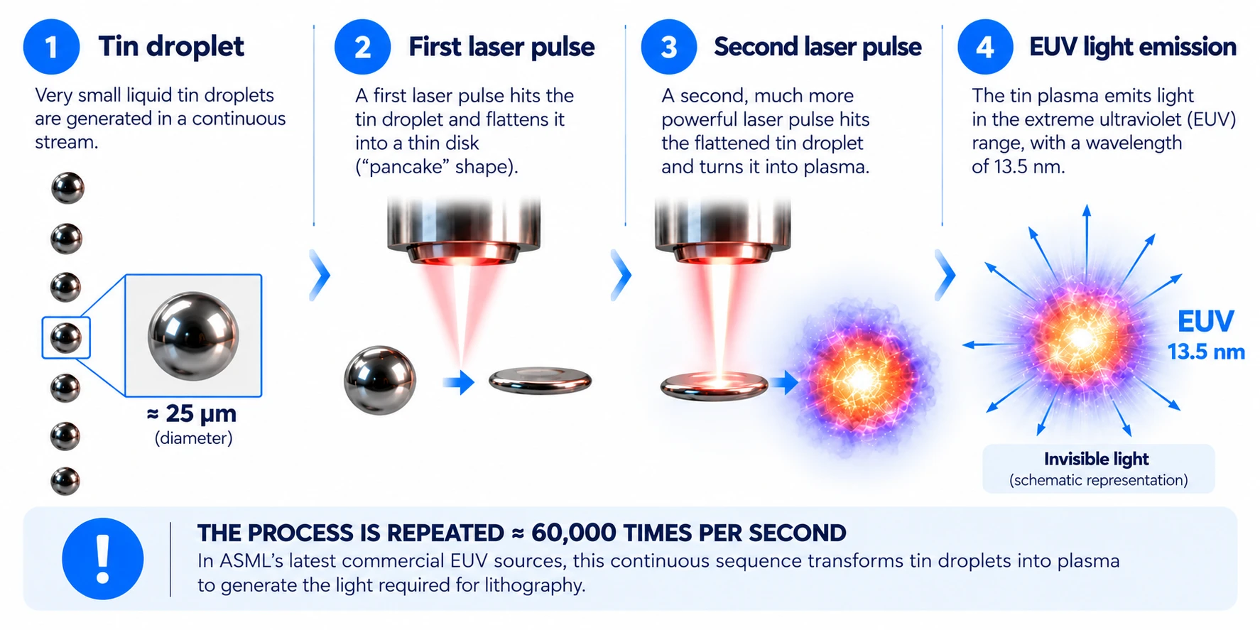
In ASML’s systems, everything begins with tiny droplets of molten tin.
They are approximately 25 micrometers in diameter and travel at roughly 70 meters per second.
A first laser pulse strikes each droplet and flattens it.
A second, more powerful pulse turns it into plasma.
That plasma then emits EUV light at a wavelength of 13.5 nanometers.
In ASML’s latest commercial EUV sources, this operation is repeated approximately:
60,000 times per second.
The challenge is not simply to generate EUV light in an experiment.
It is to produce it continuously, with enough power and stability to supply an industrial machine.
And even once that light has been generated, the problem is far from solved.
EUV Requires an Entirely Different Optical System
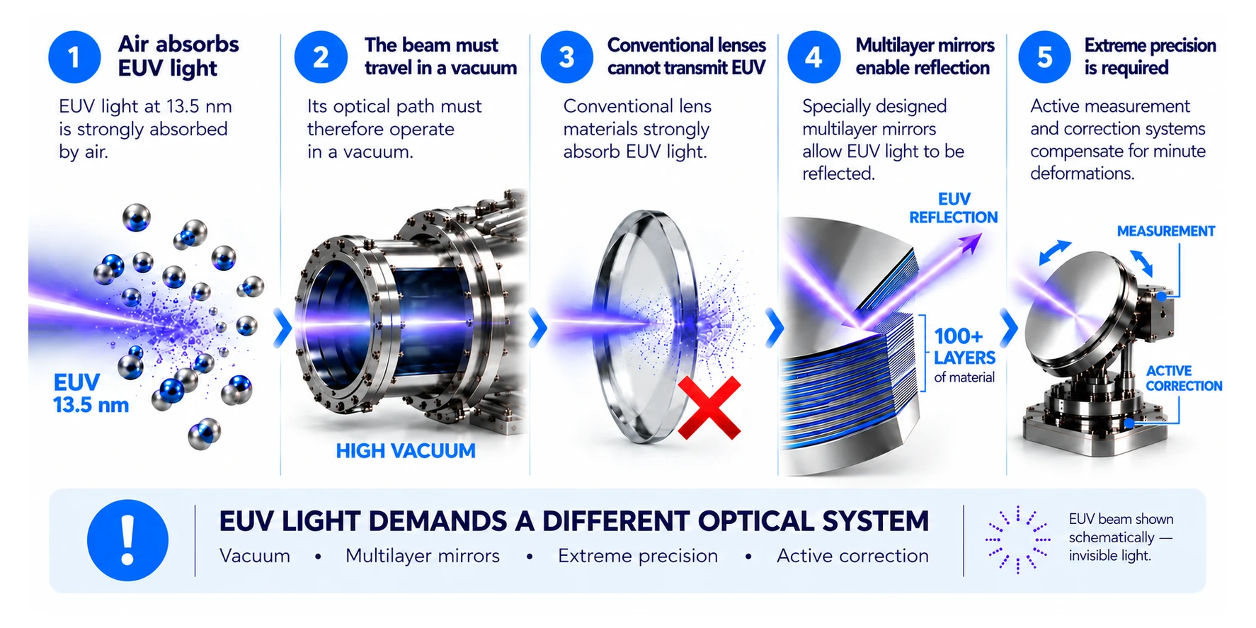
EUV light is absorbed by almost every material.
Even air presents a problem.
The optical path must therefore operate in a vacuum.
Conventional lenses are not a solution either: their materials would absorb EUV light.
Working with its strategic partner ZEISS, ASML therefore uses an architecture based on specially designed multilayer mirrors that reflect it.
Each mirror contains more than 100 layers of material.
Its surface is polished to a roughness smaller than the thickness of an atom.
But that precision must also be maintained while the machine is operating.
Light pulses heat the optics and cause minute distortions. Changes measured in millikelvins and nanometers can already affect the patterns produced on the wafer.
Thousands of actuators make minute adjustments to compensate for these effects.
The machine must continuously measure and correct its own operation.
The Challenge Is Not One Technology — It Is Their Integration
Even an EUV source and mirrors capable of reflecting its light are not enough to build an industrial machine.
The source must produce sufficient light.
The optics must control it.
The reticle and wafer must move with extreme precision.
Vibrations and temperature changes must be measured.
Errors must be corrected.
Software must coordinate everything.
And all these operations must be repeated at a pace compatible with semiconductor production.
This is where an essential part of ASML’s advantage lies.
The company has not merely accumulated individual technologies.
It has developed the ability to integrate them into a single industrial system.
And it has not done so alone.
ASML Built an Ecosystem Around the Machine
Optics provides one of the clearest examples.
ASML has worked for decades with ZEISS, its strategic partner for lithography-system optics.
That relationship became important enough for ASML to acquire an indirect 24.9% stake in Carl Zeiss SMT in 2017, following an agreement that valued the stake at €1 billion. One objective was to align the two companies on the development of EUV and its High NA generation.
The light source tells a similar story.
In 2013, ASML acquired Cymer, a US manufacturer of light sources, in part to accelerate EUV development.
Over time, ASML has brought together its own technologies, capabilities acquired through acquisitions and highly specialized partners.
For a competitor, knowing how EUV works in principle would therefore not be enough.
It would need to reproduce or replace those capabilities, then integrate them into a machine reliable and productive enough to operate every day in a semiconductor factory.
Decades to Move From the Laboratory to the Factory
Time is another part of the challenge.
ASML describes its EUV development as the result of roughly 25 years of engineering advances.
During that period, it was not enough to demonstrate that the technology worked.
The company had to increase source power and improve the optics, precision, availability and, above all, system productivity.
That distinction is fundamental.
A technology can work in a laboratory without being capable of processing wafers day after day in a factory.
Capital can fund new teams, equipment and research.
But it cannot instantly recreate the design cycles, setbacks, improvements, supplier relationships and integration experience accumulated over decades.
And throughout that time, the technology itself continues to evolve.
With High NA, ASML Is Already Moving the Frontier
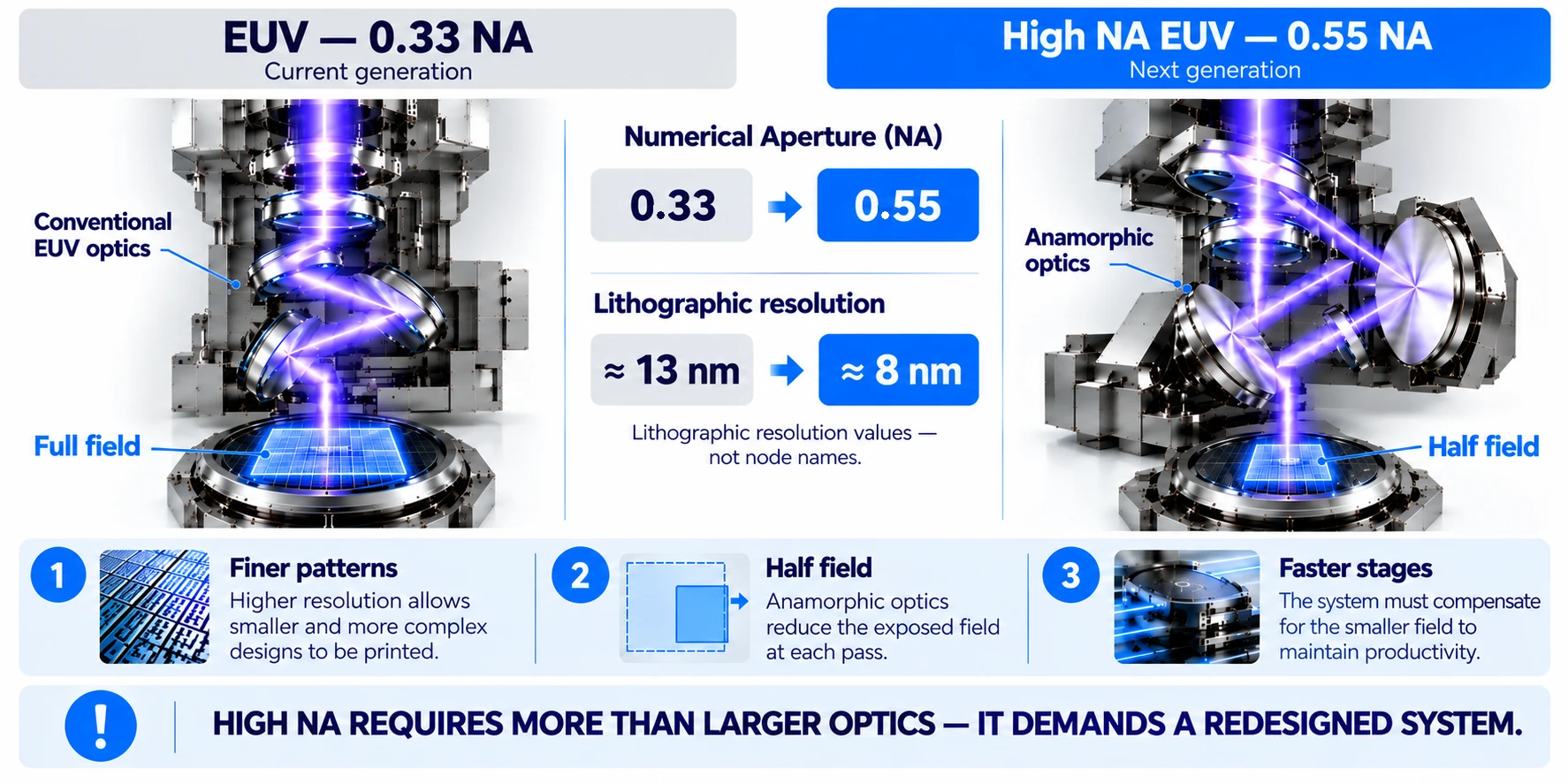
NXE EUV systems use a numerical aperture of:
0.33.
The new EXE platform, known as High NA EUV, increases that to:
0.55.
The EXE:5000 achieves a lithographic resolution of 8 nm. ASML states that, compared with NXE systems, it can print features 1.7 times smaller in a single exposure, potentially enabling 2.9 times greater transistor density.
But moving from 0.33 to 0.55 is not a matter of replacing one component.
The new optics are anamorphic. Their exposure field is half the size of that in NXE systems.
ASML therefore had to develop faster wafer and reticle stages to preserve system productivity.
In other words, improving one fundamental characteristic of the machine requires other parts of the system to be redesigned.
This is precisely the challenge EUV has presented from the beginning:
Every advance in one technology creates new constraints for the others.
An Advantage That Still Absorbs Billions of Euros
ASML invested:
€4.7 billion in R&D in 2025.
That compares with €4.3 billion in 2024, an increase of 9.2% based on the reported figures.
These investments cover areas including NXE and EXE EUV systems, future lithography generations, metrology, e-beam inspection and software.
This figure does not mean that a competitor could never develop comparable technology.
It shows instead that the technology a competitor would need to catch up with continues to receive billions of euros in research and development every year.
And despite its strategic importance, it is manufactured in extremely small volumes relative to the markets it helps serve.
In 2025, ASML reported sales of 535 systems across its system categories, including just 48 EUV systems.
A technology used to manufacture some of the world’s most advanced chips therefore depends on a relatively small number of extraordinarily complex machines.
Why Is This Technology So Difficult to Replicate?
It would be an overstatement to claim that ASML’s position is impossible to replicate, or that it will remain unchanged forever.
But EUV helps explain why certain technological leads are exceptionally difficult to close.
A competitor would not need to solve just one problem.
It would have to master EUV light generation, multilayer optics, vacuum systems, ultra-precise motion, metrology, thermal control and software.
It would need to build or replace a supplier network capable of manufacturing components to the necessary tolerances.
Then it would have to integrate everything into a machine reliable and productive enough for use in a semiconductor factory.
And it would have to do all of this while the benchmark technology continued to advance.
What makes ASML difficult to replicate is therefore not one isolated invention.
It is the accumulation and integration of interdependent technologies developed over several decades.
Key takeaways
- ASML does not manufacture chips. Among other products, it supplies lithography systems that print patterns onto silicon wafers.
- EUV uses light with a wavelength of 13.5 nm, compared with 193 nm for ArF DUV systems.
- Generating that light is itself a challenge: laser pulses turn tin droplets roughly 25 µm in diameter into plasma.
- EUV requires a different optical architecture: vacuum systems, mirrors with more than 100 layers and surfaces polished to sub-atomic-scale roughness.
- The central difficulty is integrating the light source, optics, mechatronics, metrology and software with a network of specialized partners.
- High NA raises numerical aperture from 0.33 to 0.55, but also requires new optics and stages.
- ASML invested €4.7 billion in R&D in 2025.
Conclusion
ASML’s position is often summarized in one sentence: the company builds the EUV machines used to manufacture some of the most demanding layers in advanced chips.
But that statement does not explain why those machines are so difficult to replicate.
The challenge does not lie in a single component.
It lies in the ability to generate 13.5 nm light, control it in a vacuum with extraordinarily precise optics, move and measure components at minute scales, continuously correct errors and make all these technologies work together at the productivity levels required by a factory.
ASML built that capability over decades through its own teams, acquisitions and a network of specialized partners.
And while EUV is now used in industrial production, the company is already developing High NA.
Replicating ASML, then, is not simply a matter of rebuilding a machine. It means reproducing an entire technological system — while that system continues to evolve.
Sources
This analysis draws primarily on ASML’s official technical and financial publications, including its Annual Report 2025, as well as the company’s documentation on EUV lithography, optics and the High NA platform. These sources support the principal technical, industrial and financial figures cited above.
- ASML — Annual Report 2025. investor.asml.com — R&D, system sales, 2025 operating data and EUV development.
- ASML — Light & lasers. asml.com — DUV/EUV wavelengths and the EUV light source.
- ASML — Lenses & mirrors. asml.com — EUV optics, multilayer mirrors, precision and High NA principles.
- ASML — TWINSCAN EXE:5000. asml.com — High NA platform, numerical aperture, resolution and anamorphic architecture.
- ASML and ZEISS — ZEISS and ASML Strengthen Partnership for Next Generation of EUV Lithography (press release, 3 November 2016, filed with the SEC). sec.gov — ASML–ZEISS partnership, Carl Zeiss SMT investment and High NA development.
- ASML — ASML to Acquire Cymer to Accelerate Development of EUV Technology (17 October 2012) and ASML Completes Acquisition of Cymer (30 May 2013), press releases filed with the SEC. sec.gov · sec.gov — Stated purpose of the acquisition (accelerating EUV development) and completion of the merger on 30 May 2013.